

Last month, Anwar Ibrahim, Prime Minister of Malaysia, revealed in a Facebook post that Intel is expanding its chip manufacturing facilities in Malaysia, which were first established in the 1970s. Ibrahim said Intel Foundry chief Naga Chandrasekaran had “outlined plans to begin the first phase” of expansion, which would include advanced packaging.
“I welcome Intel’s decision to begin operations of the complex later this year,” a translated version of Ibrahim’s post read. An Intel spokesperson, John Hipsher, confirmed that it is building additional chip testing and assembly capacity in Penang, “amid growing global demand for Intel Foundry packaging solutions.”
package store
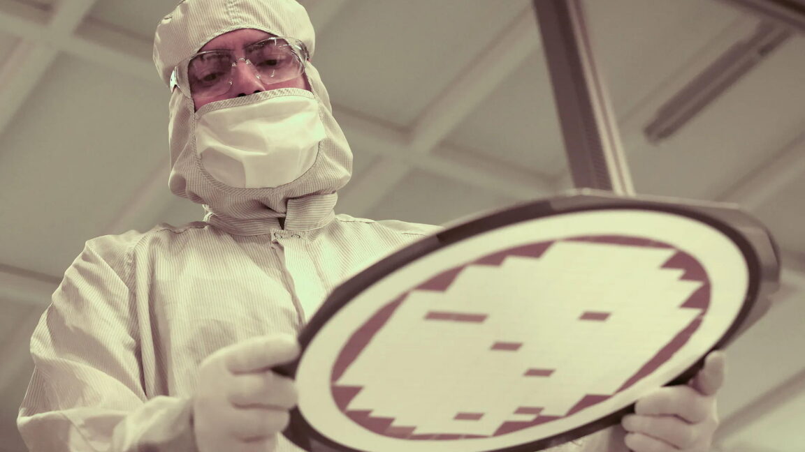
According to Chandrasekaran, who took over Intel’s foundry operations in 2025 and spoke exclusively to WIRED while reporting this story, the term “advanced packaging” itself didn’t exist a decade ago.
Chips have always required some type of integration of transistors and capacitors, which control and store energy. For a long time, the semiconductor industry focused on miniaturization, or reducing the size of chip components. As the world began to demand more from its computers in the 2010s, chips began to become even more dense with processing units, high-bandwidth memory, and all the necessary connective parts. Over time, chipmakers began to adopt a system-in-package or package-on-package approach, in which multiple components were stacked on top of each other to squeeze more power and memory from the same surface space. 2D stacking gave way to 3D stacking.
TSMC, the world’s leading semiconductor manufacturer, began offering packaging technologies such as CoWoS (Chip on Wafer on Substrate) and later SoIC (System on Integrated Chip) to customers. Essentially, the argument was that TSMC would handle not only the front end of chip manufacturing (the wafer part), but also the back end, where all the chip technology would be packaged.